


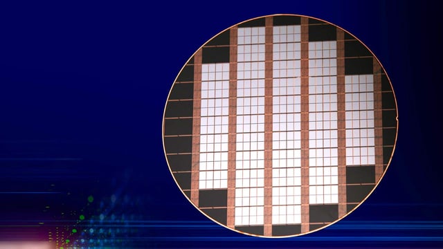
An “angstrom chip” refers to semiconductor technology featuring transistor features measured in angstroms rather than nanometers , specifically representing nodes smaller than 10 angstroms, which signifies a new era of manufacturing
Key Aspects of Angstrom-Scale Chips
- Measurement: 1 angstrom is equal to 0.1 nanometers (10 angstroms = 1 nm). Therefore, a 12-angstrom chip refers to a 1.2-nanometer process node.
- Significance: It marks a shift from measuring features in nanometers to angstroms, allowing for roughly 10 times the density of current 3-nanometer chips.
- Performance: These chips are designed to reduce electron leakage and increase power efficiency for advanced AI and high-performance computing. [1, 2, 3, 4, 5]
Industry Development & Timelines
While leading foundries are currently focusing on 2nm and 1.4nm (14A), the roadmap extends to 1.2nm (12A) and beyond: [1, 2, 3]
- Intel (14A/10A): Intel has already begun pioneering the “Angstrom Era” with its 18A (1.8nm) and 14A (1.4nm) processes, utilizing High-NA EUV lithography to create smaller, denser transistors.
- TSMC (1.4nm & Beyond): TSMC is advancing through its 2nm process and is expected to move into 1.4nm (A14) and potentially 1.2nm, with industry analysts estimating high costs per wafer for these advanced nodes.
- Technology Shifts: Achieving these sizes requires new transistor architectures like Gate-All-Around (GAA) and backside power delivery (PowerVia), which are already entering production in 2026. [1, 2, 3, 4, 5, 6]
Enabling Technologies
- High-NA EUV Lithography: ASML’s Twinscan EXE:5200B machines are essential for manufacturing these chip sizes, allowing for 8nm resolution.
- New Materials: Moving beyond traditional silicon to 2D materials like graphene and transition metal dichalcogenides (TMDs) is crucial for managing electrons at the sub-nanometer scale.
- 3D Stacking: Using advanced packaging and chiplet designs to stack, rather than just shrink, components is expected to be a primary driver of performance, as explored by organizations like imec. [1, 2, 3, 4]
Democracy is a Bond 1977
Star Wars 1977
Professor Miller 1973